The premise behind the Generation 7 RepRap electronics is replicability, so we decided to fabricate our own for our Huxley in progress. Originally we had hoped to set up our Mendel for milling with our Dremel, but with our sticky y axis problem being only improved but not completely solved by increasing the belt tension, we decided to play it safe and etch the PCB instead.
Maplin sells a Student PCB Etching Pack that was perfect to get us started, complete with tray, etch resist pen, copper clad board and ferric chloride:
Preparing the PCB design for etching
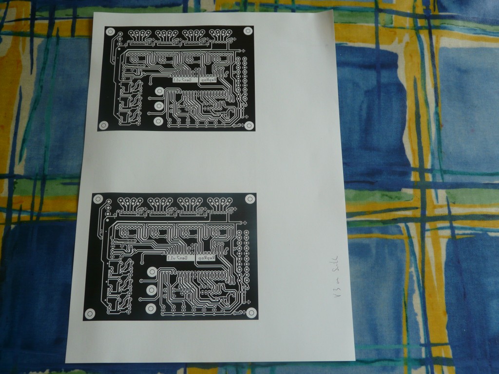
First step in etching the Gen 7 PCB was to prepare the PNG image of the board. Gen 7 uses an Open Source electronics design package gEDA and there is advice on preparing the board for etching on the wiki page. gEDA took a little getting used to, but it turned out pretty easy to follow the instructions and export the required PNG file.
I added the ground plane, and widened the tracks. We have a Dremel and Workstation 220 , and bought the 7 Piece Precision Drill Bit Set 628 which come in sizes 0,8 / 1,2 / 1,6 / 2,0 / 2,4 / 2,8 and 3,2 mm and the necessary collets. These don’t match exactly the hole sizes in the Gen 7 design, so I also resized the holes and pads for these drills.
Pen Plotting or Toner Transfer?
We have a working Mendel, so pen plotting would be the obvious choice for transferring the PCB design in etch resist onto the board. The wiki even has a helpful page dedicated to Pen Plotting with a couple of different methods. Good stuff!
…or so I thought. I spent a good day trying and failing to make progress on generating the GCode to plot the PCB design with our Mendel, working through the different suggested methods on the wiki page:
- The version of RepRap Host and firmware we are using does not have the PCB plotting functionality, and seeing as it is working I didn’t fancy an upgrade going wrong. Not to mention I have no idea how to export the Gen 7 PCB design as the Gerber files required by the RepRap Host using gEDA.
- Using Inkscape to convert the PNG to SVG for use with Skeinforge seemed to be working, until I realised that it was plotting the negative of the design! Not being au fait with Inkscape I didn’t know how to invert the paths and spaces.
- Cad.py was the most promising, but it just kept crashing the computer before it had finished generating the GCode.
These problems would probably be trivial to solve for someone familiar with gEDA or Inkscape, but as this was the first time I was using them and being conscious of considerable time passing trying to troubleshoot it seemed far simpler to cut my losses and go with the quick and dirty toner transfer method.
Toner Transfer
Dad’s office has several laser printers, and on the advice of Andy Kirby’s article on “How to Make Good Quality Single Sided PCB’s” we bought some silk paper from Ryman and printed a couple of copies out. Turns out the ones printed on the colour printer have much more even and darker blacks, and so transfer better and are more etch resistant.
I would definitely recommend printing out at least twice as many copies as you think you’ll need. Even following Andy’s instructions, it took several attempts at ironing on the design and soaking off the paper in water only to clean the poor results off with acetone and start again before we got a decent transfer. This was probably due to having the iron at the wrong temperature, missing some areas or being too vigorous and moving the paper whilst ironing the first couple of times before we got the hang of it.
Etching
The etching was a pretty simple affair, involving wearing some fetching goggles, marigolds and old clothes. Most of the exposed copper was removed quickly but there were a few stubborn areas that got us in trouble for being late for dinner. In the rush to tidy up there were two things we failed to notice:
- Some ferric chloride had splashed through the slats in the garden table onto my feet, leaving me with orange patches on my feet for the next few days.
- The bottle cap on the ferric chloride wasn’t on properly.
Unfortunately we only discovered the latter a few days later.
Drilling the holes
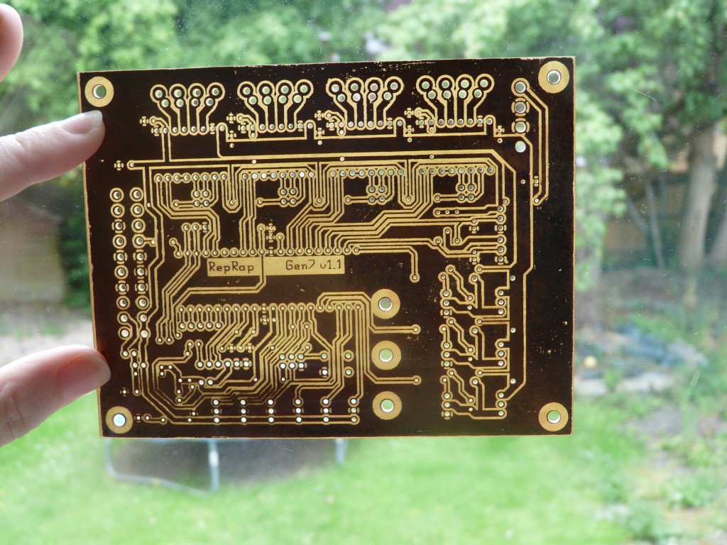
With our aforementioned Dremel and Work Station set up this was a straightforward but fairly time consuming task. It was delayed a few days however by the wrong size collet being supplied in our order, but the end result was pretty pleasing.
Tarnishing
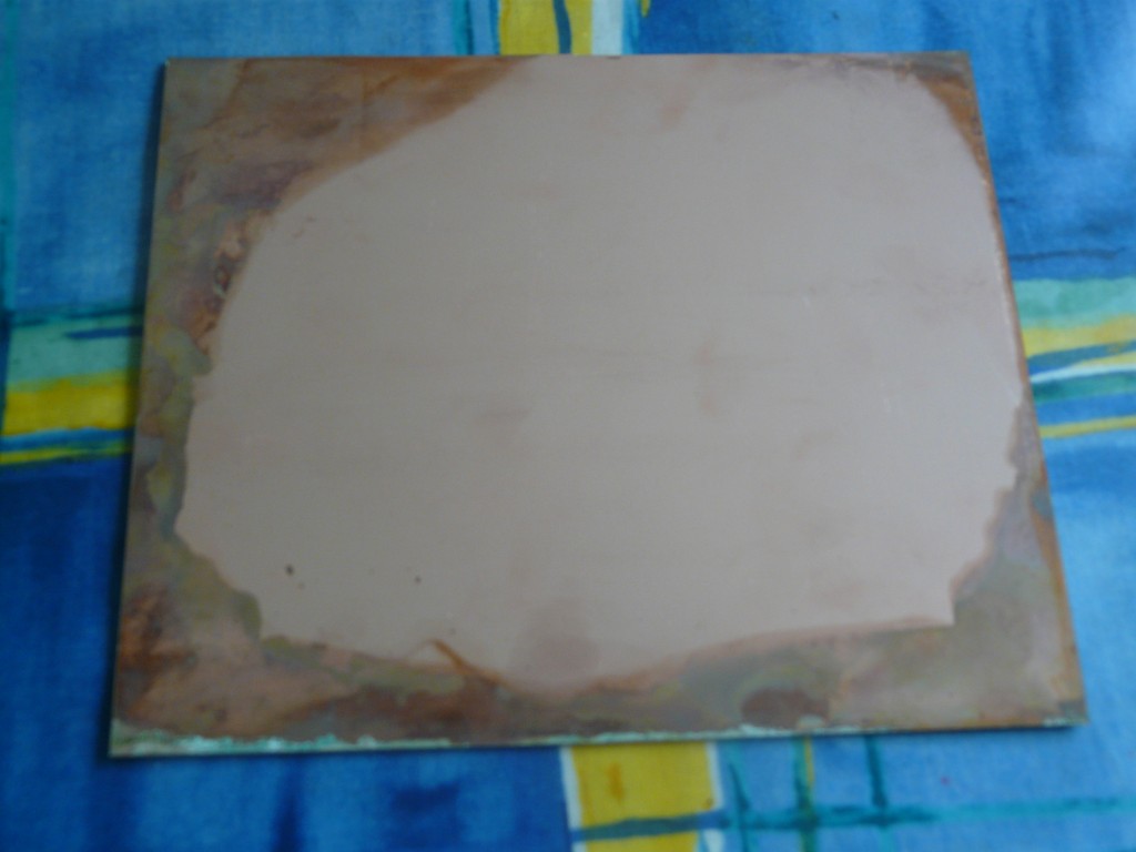
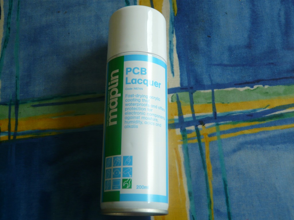
In that time, the copper had begun to tarnish so we decided to chalk that board down to experience and make a fresh one once we had ordered all the components to solder on to the PCB, investing in some PCB lacquer again from Maplin to prevent the new board tarnishing.


